The New “Shift-Left” Multi-Dimensional PCB Design-Verification Platform
A “shift-left” PCB design verification solution within the engineer’s authoring environment is the industry’s first of its kind, claims developer Mentor, a Siemens business. This new Xpedition platform helps the designer develop accurate virtual prototypes earlier in the design flow, to validate their designs with ease while reducing design re-spins.
To find out more about this latest tool, I talked with David Wiens, Xpedition product marketing manager for the Electronic Board Systems segment of Mentor.
David Wiens, Xpedition Product Marketing Manager, Electronic Board Systems, Mentor
What was the basis for this new technology development since Mentor currently has a broad portfolio of PCB design solutions?
This new PCB design platform is focused on multi-dimensional verification—a critical area that’s lacking in sufficient technologies. The systems design industry continues to increase with global pressures to deliver advanced products in shrinking time-to-market windows. In our conversations with customers, PCB design managers are challenged by the lack of robust verification tools, or available tools that are too difficult to use. Increasing performance requirements plus the pressure to improve product quality are driving these teams to look at alternative approaches to their current verification methods with physical prototypes.
Best-practice design processes validate a “digital twin,” or model, of the design, early and often to minimize re-spins and shorten design cycles. Our solution is a “shift-left” PCB design flow that allows design engineers and layout designers to validate within their native environment, removing the bottleneck of specialist reviews later in the design process.
We met with industry analyst Chad Jackson of Lifecycle Insights, who recently published a study on electronics simulation-driven design and its correlation to re-spins, costs, and time-to-market. His findings support our new technology, enabling PCB design teams to simulate earlier and often—minimizing critical issues in the early stages of product development.
What are some of these findings from the Lifecycle Insights study?
Lifecycle Insights reports that 58% of all new product design projects incur added costs and time delays. And 75% is worst case—where projects are cancelled for various reasons, including project delays or reallocated resources.
The study includes the high cost of design failure by looking at re-spins and re-designs due to errors found in physical prototypes and production boards. The average design re-spin averaged 8.5 days to complete at a cost of $44,000 (USD) per re-spin. The study reports an average of 2.9 re-spins per project. So this amounts to $127,000 or more per design—that’s substantial. Today’s high-end designs can approach six figures for a re-spin, and with steadily increasing design complexity, I foresee the number of re-spins and associated costs increasing year over year.
That’s interesting. Tell me more about what Mentor is doing to address this issue.
It may be worth discussing the conventional PCB design processes first. Traditional processes leave validation for the prototype lab, so it’s difficult to know the root cause of what caused the problem and options to remedy the problem. There are analysis tools in the market, and these are used right before prototype. But this approach relies on specialists trained to use these complicated tools, which can become a “bottleneck,” particularly with time-to-market deadlines.
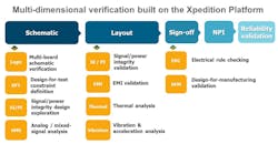
With the Xpedition design verification platform, validation is implemented as early as possible in the design process. This “shift-left” approach is applied right after an error could be made in the system definition, schematic, or layout stage. Design validation is handled by the author at that stage, such as the design engineer during the schematic stage, or the layout designer at the layout stage. We tightly integrated our validation tools with the authoring environment, making them easy to use.
The Mentor Xpedition PCB design platform provides the industry’s first “shift-left” upfront verification capability within the engineer’s authoring environment to minimize design re-spins and improve overall product quality.
Validating during the design process is often referred to as virtual prototyping, leveraging a “digital twin” model of the design. And by validating first-order issues during design authoring, the specialists can focus on more complex, complete multi-physics analysis for the challenging parts of the design versus the entire design. The net result is a shortened design cycle with reduced re-spins that lead to higher-quality products, validated by the respective design authors. Mentor is the first PCB design software company to provide this “shift-left” verification capability.
Can you elaborate on specific capabilities for upfront design analysis? For example, what can the design engineer do to validate the schematic design?
Based on our broad portfolio of analysis and verification technologies, the design engineer can identify the most common schematic integrity errors before layout. Traditionally, this is a manual, peer review process to catch errors, which is not only time-consuming but prone to miss mistakes.
We can conduct more than 150 voltage-aware rule checks automatically, on every net in the system design including across multiple boards—essentially hundreds of thousands of checks per design. Automated checking can uncover problems with improperly connected components, missing power or maximum power exceeded on a component, improperly placed diodes, pin voltage mismatching, missing connections, nets missing the receiver, wrong board-to-board connections, as examples. Even the smallest schematic error can lead to a major system failure.
Are there any customers who are realizing the benefits of this capability that you can talk about?
A major mil-aero customer uses Xpedition, and they were able to identify 13 critical errors that reduced their debug time from two months to two weeks, not including their time to actually re-design their system. By replacing the manual process with automated schematic analysis, this customer was able to review 100% of the nets for assured coverage.
Our tool provides color-coded results to highlight critical errors from possible defects—including basic warnings to improve the design. If an error is incorrectly identified, the user can hide it or omit it from future verification checks. Another benefit with this schematic analysis tool is seamless integration. The bill-of-materials (BOM) and netlist data are automatically extracted and results reviews are cross-probed into the schematic. With a library comprising over six million parts, coupled with fast modeling services, tools adoption and ease-of-use are clear advantages. We have found among our customers that this capability has saved them an average of 18 days per project.
What are some of the other new capabilities for “shift-left” verification?
Integrated testability analysis. Test point assignment and test coverage are usually considered late in the PCB design process. Typically, the first or second revision of the product will be completed before testability issues are considered, but test strategy optimization is difficult at this stage since all design constraints were considered during layout. Therefore, testability considerations should be made during schematic capture, driving test point requirements during layout.
During layout, the test strategy is validated, so this capability can identify errors early and reduce errors associated with insufficient test coverage. By defining appropriate test coverage, resulting in not too many and not to too few test points, this solution makes design hand-off to manufacturing much more seamless, reducing expensive costs during functional testing. This “manufacturing-aware” feature delivers an efficient flow, from design conception to manufacturability.
You mentioned “multi-dimensional verification” earlier during our conversation. What do you mean by this?
The new Xpedition platform includes improved integrations of our existing tools for “shift-left” verification. These include automated component modeling for vibration and acceleration simulation, integrated electrical rule checking, DC drop for multi-board and rigid-flex designs, and concurrent design-for-manufacturing (DFM) analysis during layout. As the market share leader in PCB design technologies, Mentor provides the most comprehensive set of verification technologies within the Xpedition flow. We believe this new platform will result in higher-quality products while saving time and costs by mitigating design re-spins.
Are there any additional points you wish to share on this new solution, Dave?
We’ve developed several items that your readers may want to explore. A new white paper on this subject that also references the Lifecycle Insights research highlights, and an archived webinar on this new “shift-left” verification platform. They can be found at www.mentor.com/pcb/xpedition.
David Wiens is the Xpedition product marketing manager for the Electronic Board Systems segment of Mentor, a Siemens Business. He joined Mentor in 1999 through the acquisition of VeriBest. Over the past 25 years, he has held various engineering, marketing, and management positions within the EDA industry. His focus areas have included advanced packaging, high-speed design, routing technology, and integrated systems design. He holds a B.S. in computer science from the University of Kansas.


